Introduction
I recently purchased a discount VLP-32 LiDAR sensor off eBay.
Unfortunately, the sensor didn’t come with the Interface box required to communicate with the sensor.
I could spend another USD 200 on a new one or design one of my own.
While this was a relatively simple project, it’s helpful to talk through the steps I took to go from an idea to a working solution. The schematics and PCB layout are available here.
Requirements
Starting with the documentation provided by Velodyne, I identified the critical components, which I needed, in order of priority.
Protect the LiDAR using a fuse and a Transient Voltage Suppression (TVS) Diode. Provide power to the LiDAR. Connect the LiDAR to Ethernet.
Velodyne’s circuit design includes a 5V voltage regulator so that a GPS receiver can easily be integrated to provide precision timing. I removed this functionality to reduce complexity and risk.
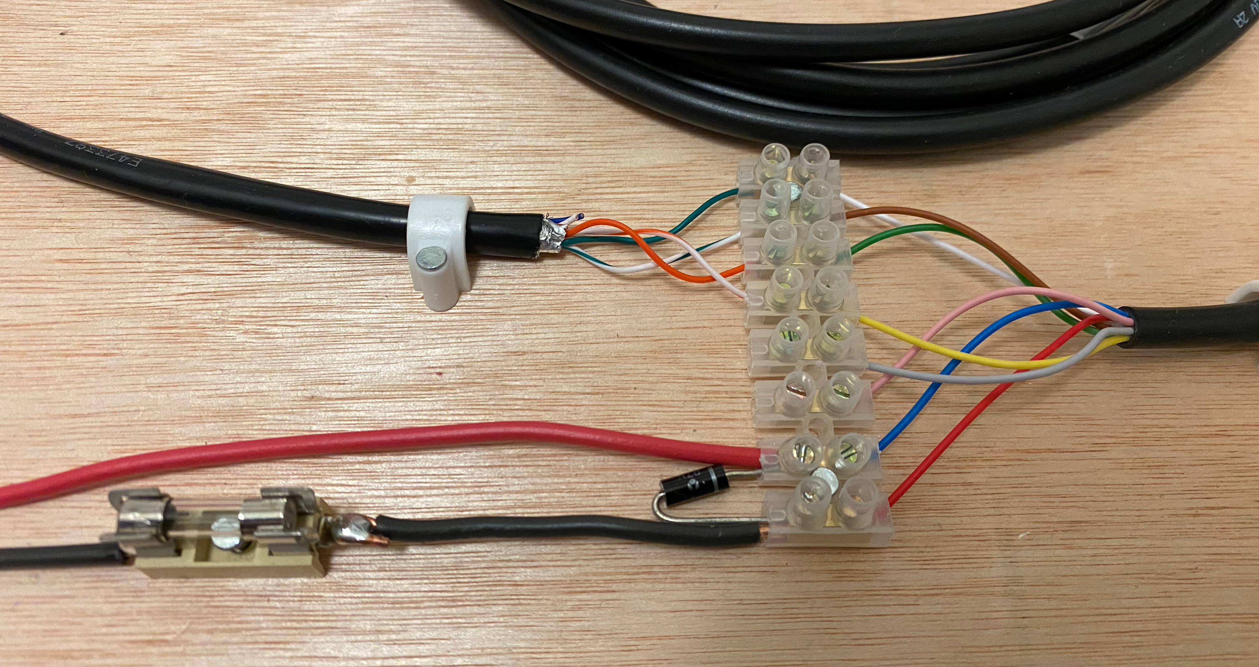
Before starting, I laid out a potential circuit with wires and plywood as a sanity check.

Design
Schematic
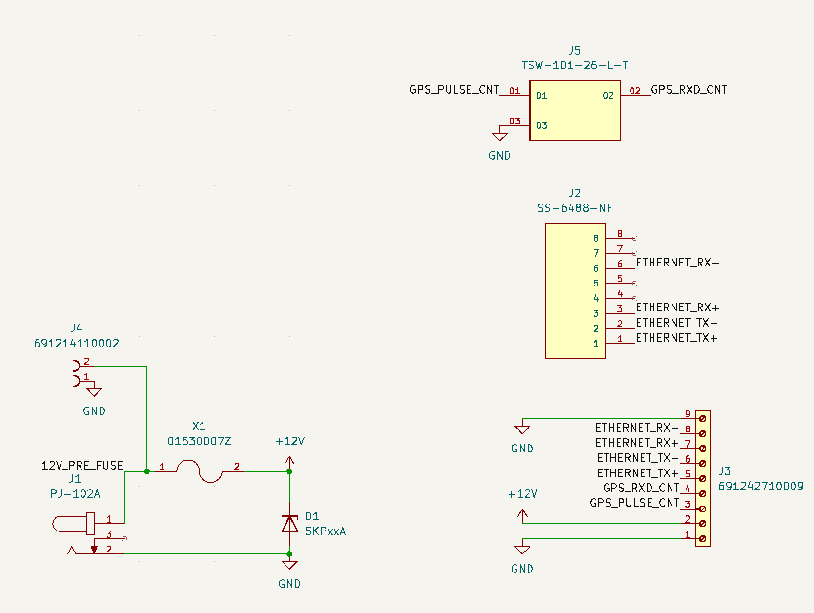
I used the open source KiCAD to sketch a schematic, a logical representation of how all the different components are connected.
At this stage, I used Mouser to find components that suited my needs, and then SnapEDA to download the symbols, footprint and 3D model of the component. 
Layout
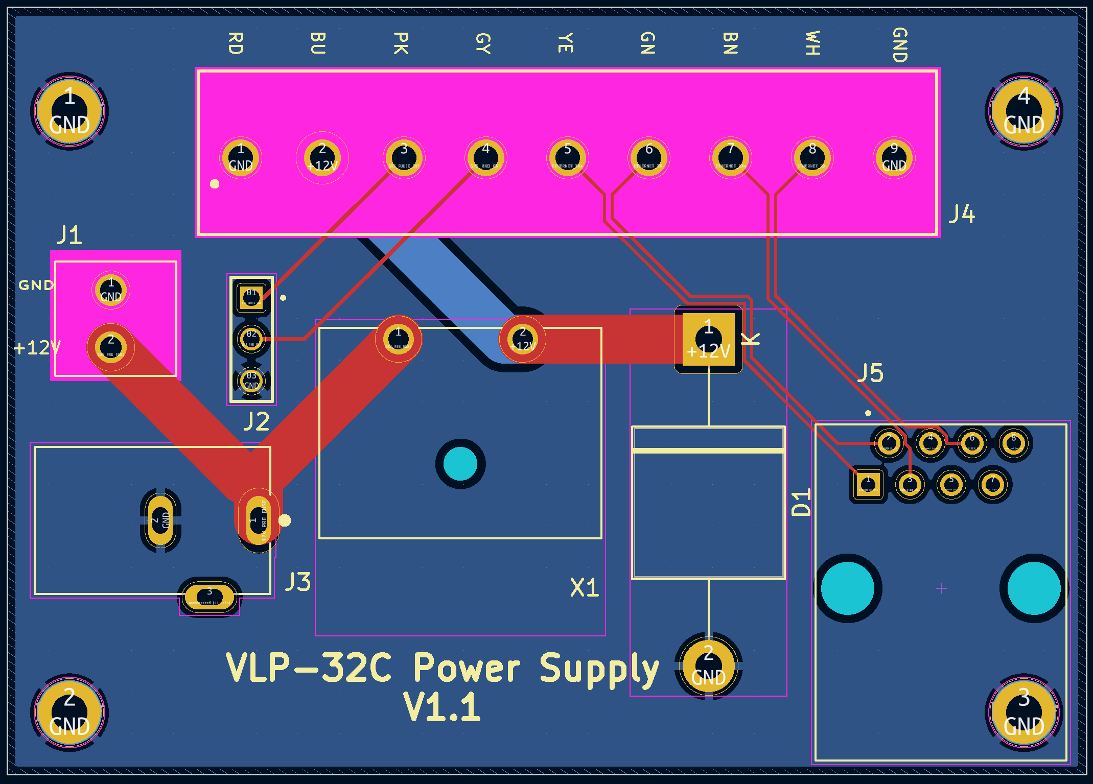
Now that we have a completed logical circuit with components, we have to lay them out on a PCB. The PCB is the physical manifestation of our schematic, physically connecting the components.
This is a fascinating exercise because we are simultaneously balancing many different constraints. If you want to learn more, the Routing page on Wikipedia is a great place to start.

Once the layout is completed, we can visualise the layout of all the different physical components.

Fabrication
Now that we have a design for our PCB, it’s time to get it fabricated. I chose JLCPCB. Total cost ±2 euros per PCB, shipping and taxes included.
For components, I used Mouser. The total cost for the components was approximately ±10 euros per PCB.
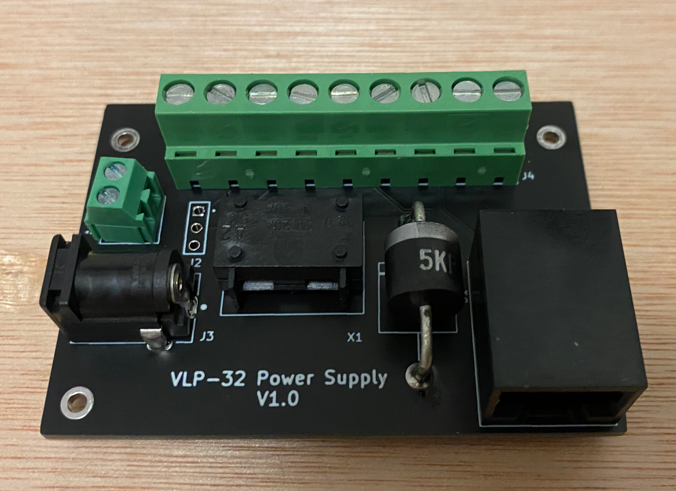
Finally, it’s time to solder the components to the board, giving us our finished product.

Conclusion
The PCB was functionally a success, but I want to reflect on what I got wrong: The size of the PCB: I should have targeted a standard enclosure size. The size of the text on the PCB. It’s too small, an error I have now fixed. Using different-sized wiring blocks.
The PCB and Components are available here; if you have a VLP series LiDAR, you feel very trusting, please go ahead and make your own interface circuits.